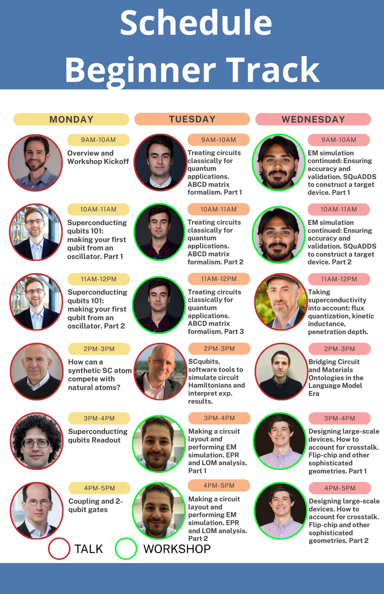
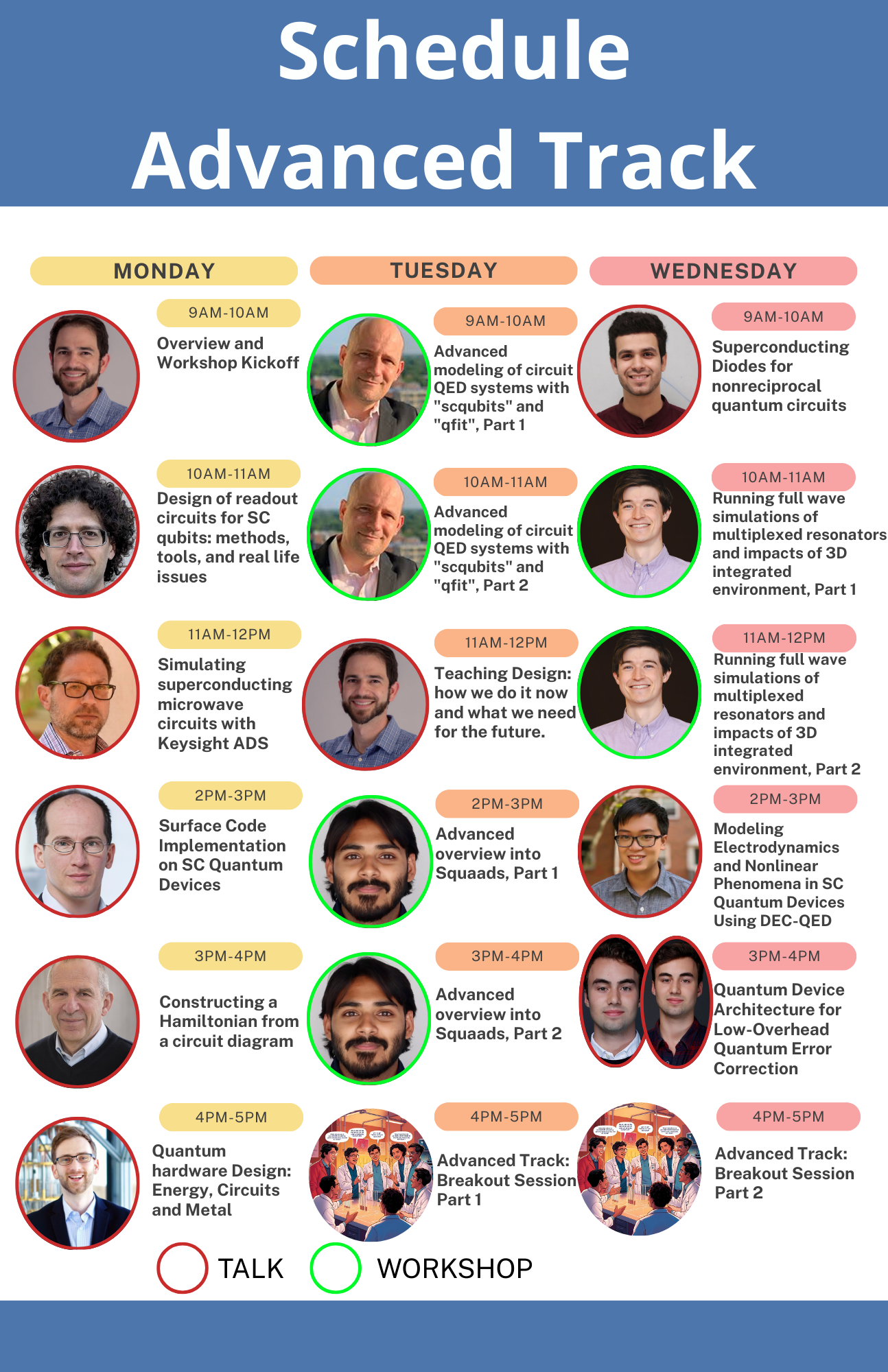
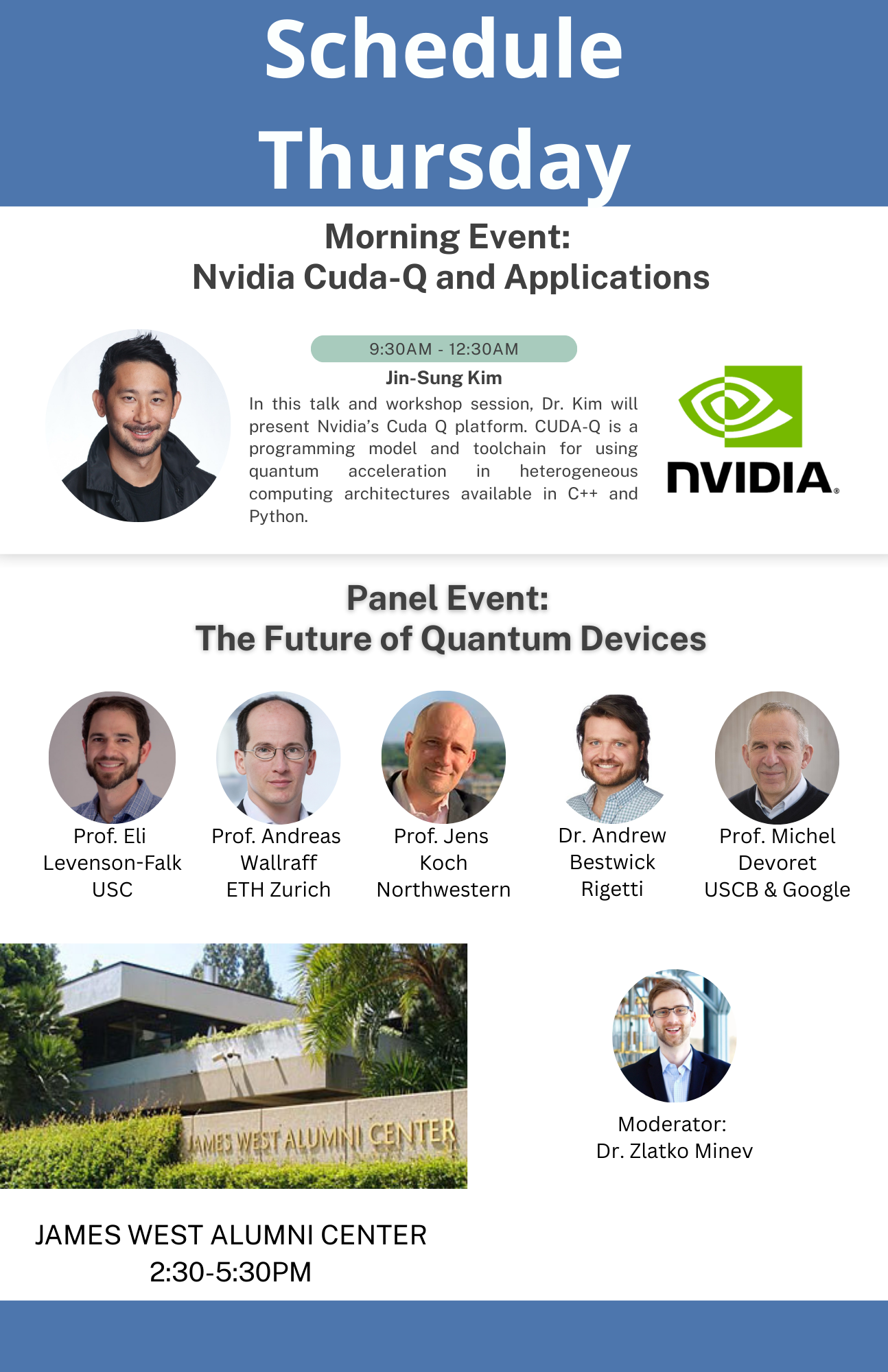
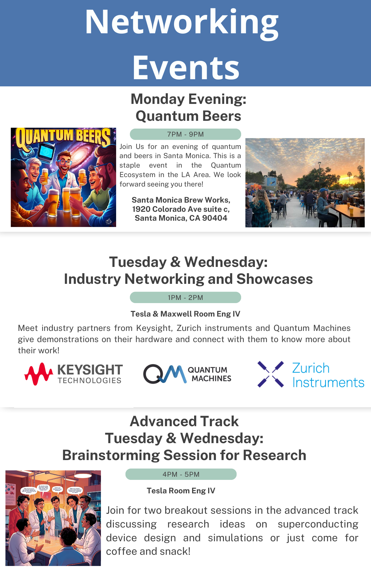
Program Schedule
The Quantum Device Workshop will be held from May 19th to May 22nd at UCLA.
There will also be an option for online attendance as well.
The content of the workshop can be found below. There will be 3-4 speakers each day.
You can find a detailed schedule for each track here. Assignment to speaker to time slots are subject to change until May 1st.
Beginner Track
Day 1: Foundation
Review classical LC circuits, resonance, and transmission lines
Circuit quantization, the Josephson junction, and transmon qubits
Introduction to circuit QED and dispersive interactions
Day 2: Theory
Charge and flux drives and single-qubit gates
Qubit-qubit coupling and two-qubit gates
Readout, SNR, and Purcell effects
Day 3: Design
Design circuit Hamiltonians
Perform EM simulation and learn layout generation tools
Interpret EM simulations (LOM and EPR)
Day 4: Non-idealities and more
Quantum and classical crosstalk, crosstalk suppression techniques
Interface dielectric loss and suppression techniques
Advanced designs, including flip-chips, through-silicon vias, and multi-chip-modules
Advanced Track
The Advanced Track is highly subject to change; we hope to tailor it to the enrollees.
Day 1: Introduction
Review of essential topics in superconducting quantum devices, including device design, simulation, and control integration
Day 2: Advanced simulation
Finite element analysis, energy participation ratio calculations, and optimization algorithms
AI-driven approaches in simulation, automated device design processes, and intelligent control systems
Day 3: Devices
Advanced device architectures and cutting-edge applications
Complex multi-qubit systems and advanced control techniques
Day 4: Error correction
Surface code implementations and logical qubit architectures
Device layout optimization